FPGAs 3: Wishbone and Soft Cores
Sun, Aug 23, 2020 Companion code for this post available on GithubOne of the core design patterns in the arsenal of an FPGA developer is the finite state machine. Such systems can be small, fast, easy to reason about and extremely powerful for sequential logic. But there can come a point where a state machine grows so complex that the hardware implementation starts to become extremely costly, or perhaps you want to be able to update the behaviour of a large state machine from an external memory. At such a time, it may make sense to consider replacing a complex special-purpose state machine with a highly evolved general purpose state machine - in other words, a CPU.
In this post, we will cover the basic idea of what a soft CPU is, how to connect a CPU to ROM and RAM using the Wishbone bus, how to write firmware for our custom SoC, how to use interrupts, and how to build our own memory-mapped IO peripherals. This post will assume some familiarity of Verilog and C++ code; if readers are less familiar with Verilog I would recommend starting with this post that attempts to explain what FPGAs are, and how Verilog can be used to command them.
Soft CPUs
If one considers the stripped down structure of a CPU, they can start to see how a CPU is, at its core, simply a state machine - it loads an instruction, decodes the instruction, performs some operation based on the instruction, increments the program counter and transitions back to the fetch state. One could definitely have some fun creating their own minimal CPU with a custom instruction set, but the level of complexity and tooling that goes into a performance-competitive CPU is no mean feat. Thus, for someone that wants to get a system built with minimal reinvention, it makes sense to utilize one of the increasingly many CPUs available online. There are many to choose from - this article has a good rundown of some free options, and even proprietary designs such as the ARM Cortex-M0 are available for evaluation. However, the complexity of integration and licensing headaches are somewhat of a negative for ARM cores in particular. For the purposes of this article, we will focus instead on the highly customizable and increasingly popular RISC-V ISA, which boasts multiple free implementations targeting different use cases.
The shortlist
PicoRV32
One of the earliest such CPUs. Optimized primarily for small size and high max frequency, this core has weaker performance per clock cycle numbers than some other CPUs but is easy to integrate and can fit handily in even some of the smaller FPGAs on the market.
SERV
One of the more unique cores, SERV is a bit-serial architecture - by taking the tradeoff between clock cycles and design area to the extreme, this CPU executes on only one bit at a time (instead of on 32 bits at once), reducing the size of the core to the point that at least 16 cores may be instantiated on the ICE40LP8K, an FPGA with only 7680 logic elements.
VexRiscv
Of the readily available FOSS RISC-V cores, the VexRiscv is certainly the most configurable. The core itself is written using Spinal HDL, a set of Scala libraries, which allows for higher level components to be tweaked more readily than would be possible in straight Verilog. It can be tuned all the way from a minimal 500 LUT core with no hardware multiply or interrupt support all the way up to a 3000 LUT variant with caches, interrupts, branch prediction and MMU that allows one to run a full Linux core.
Customizing the VexRiscv
Given the customizability of the VexRiscv, and the superior performance per clock cycle compared to the other options, we will use it as our base for this project. The downside to customizability is understanding all these configuration options, so the first thing to do is have a read through some of the example core generation files, and write our own CPU definition to meet our needs.
If we take a look at the
demo
folder in the VexRiscv repo, we see a number of templates we can use to base
our core off. We will mostly pull from the GenFull example, and our full
custom configuration and generated CPU file can be found in the repo for this blog post
here.
If we read through our custom GenVexRiscv.scala, we can see that the CPU is constructed of various plugins. Most are named in a fairly self-explanatory way, or do not require much modification, so we will touch on only some of them directly here. The first is our ibus, or instruction data bus plugin:
// We need an instruction data bus on the CPU. This bus is separate
// from the data bus for performance reasons, and here we will
// instantiate the cached version of this plugin, which is a
// significant performance improvement on a non-cached implementation
new IBusCachedPlugin(
  // We want to be able to set the reset address in verilog later, so
  // leave it null here
  resetVector = null,
  // Conditional branches are speculatively executed.
  // There is no tracking of whether a branch is more likely to be
  // executed or not
  prediction = STATIC,
  // Include a 4KiB instruction cache
  config = InstructionCacheConfig(
    cacheSize = 4096,
    bytePerLine = 32,
    wayCount = 1,
    addressWidth = 32,
    cpuDataWidth = 32,
    memDataWidth = 32,
    catchIllegalAccess = true,
    catchAccessFault = true,
    asyncTagMemory = false,
    twoCycleRam = true
  )
),
Caching is one of the most powerful performance tools there is for CPUs, so we want to be sure to add a generous cache to our CPU here. Otherwise, non-cached instruction fetches will require us to spend at least 2 cycles asking for data over the wishbone bus. If you have to wait two cycles for each new instruction, your effective clock speed has already been cut in half! If your code is stored on external memories, such as a SPI flash, your uncached performance will be even worse as you have to potentially spend many clocks sending addresses and data back and forth over a SPI interface for each new instruction.
The next section that we want to pay some special attention to is the
CsrPlugin. The RISC-V ISA defines a number of configuration and status
registers, but it is not necessarily required that all are present, readable or
writable in a given implementation. We will want to make our CPU flexible when
it comes to interrupt configuration,
and we would also like to be able to use the cycle counter register, so we will
configure registers mtvec and mtcycle with READ_WRITE access.
We could also set some CPU
identification registers here, if for example our firmware would run on
different flavours of soft CPU and would need to determine capabilities at
runtime.
// Implementation of the Control and Status Registers.
// We want to make sure that registers we use for interrupts, such as
// mtvec and mcause, are accessible. We have also enabled mcycle
// access for performance timing.
new CsrPlugin(
  config = CsrPluginConfig(
      catchIllegalAccess = false,
      mvendorid      = null,
      marchid        = null,
      mimpid         = null,
      mhartid        = null,
      misaExtensionsInit = 66,
      misaAccess     = CsrAccess.NONE,
      mtvecAccess    = CsrAccess.READ_WRITE,
      mtvecInit      = 0x80000000l,
      xtvecModeGen   = true,
      mepcAccess     = CsrAccess.READ_WRITE,
      mscratchGen    = false,
      mcauseAccess   = CsrAccess.READ_ONLY,
      mbadaddrAccess = CsrAccess.READ_ONLY,
      mcycleAccess   = CsrAccess.READ_WRITE,
      minstretAccess = CsrAccess.NONE,
      ecallGen       = false,
      wfiGenAsWait   = false,
      ucycleAccess   = CsrAccess.READ_ONLY,
      uinstretAccess = CsrAccess.NONE
    )
),
The final thing that we will do to this CPU is ensure that it speaks the Wishbone protocol on the instruction and data buses. Wishbone is a standard protocol for on-chip communication, and has the benefit of being very simple to implement. Luckily the VexRiscv comes with a built-in function to transform the interface to wishbone, so we simply need to invoke it:
// CPU modifications to use a wishbone interface
cpu.rework {
  for (plugin <- cpuConfig.plugins) plugin match {
    case plugin: IBusSimplePlugin => {
      plugin.iBus.setAsDirectionLess()
      master(plugin.iBus.toWishbone()).setName("iBusWishbone")
    }
    case plugin: IBusCachedPlugin => {
      plugin.iBus.setAsDirectionLess()
      master(plugin.iBus.toWishbone()).setName("iBusWishbone")
    }
    case plugin: DBusSimplePlugin => {
      plugin.dBus.setAsDirectionLess()
      master(plugin.dBus.toWishbone()).setName("dBusWishbone")
    }
    case plugin: DBusCachedPlugin => {
      plugin.dBus.setAsDirectionLess()
      master(plugin.dBus.toWishbone()).setName("dBusWishbone")
    }
    case _ =>
  }
}
When we are happy with our configuration file, we need to generate a Verilog
output we can feed to out synthesis tools. To do so, first clone the VexRiscv
repo, and install the Scala build tool sbt. Then add our generation script,
and build:
# Clone the VexRiscv repo
git clone https://github.com/SpinalHDL/VexRiscv.git
# Ensure we have the scala build tool
sudo apt install sbt
# Clone the associated code for this blog post
git clone https://github.com/rschlaikjer/fpga-3-softcores.git
# Copy our core generation spec into the VexRiscv repo
cp fpga-3-softcores/vendor/vexriscv/GenVexRiscv.scala VexRiscv/src/main/scala/vexriscv/demo/
# Move into the Vexriscv repo, and buld our core
cd VexRiscv
sbt "runMain vexriscv.demo.GenVexRiscv"
The first invocation of sbt may take some time as it resolves dependencies,
but at the end you should end up with a new VexRiscv.v at the top of the
repo. Step one is complete - we have our very own CPU.
Wishbone
Wishbone is a simple on-chip logic bus, with relatively low complexity required to implement the ‘classic’ non-pipelined interface. Other buses, such as AXI from the AMBA family of interconnects from ARM, are more powerful but come with a higher cost to implement, both in complexity and logic area. For our application, wishbone is more than sufficient.
The classic Wishbone cycle
The basic Wishbone interface consists of the following signals, some of which travel from the master to the slave (m2s) and some of which travel from the slave to the master (s2m):
wire [31:0] m2s_adr; // Address select
wire [31:0] m2s_dat; // Data from master to slave (for writes)
wire  [3:0] m2s_sel; // Byte select lanes for write enable
wire        m2s_we;  // Write enable (active high)
wire        m2s_cyc; // Cycle in progress. Asserted high for the duration of
                     // the transaction
wire        m2s_stb; // Strobe output. Asserted high to indicate data is valid
                     // for transfer from the master to the slave
wire [31:0] s2m_dat; // Data from slave to master (for reads)
wire        s2m_ack; // Read data valid strobe
The basics of a wishbone transaction are that the master must assert the
m2s_cyc
line to indicate that a transaction cycle is in progress. On the same cycle, or
any subsequent cycle before m2s_cyc is deasserted, the master may load the
address, write data, write enable and write select signals and asssert the
m2s_stb signal to indicate to the slave that these data are valid. The slave will
then perform whatever operation has been requested (read or write as according
to m2s_we), and when ready present
output data (if necessary) on the s2m_dat signal and strobe the s2m_ack
signal to indicate that the data is valid. The master may then initiate another
operation by asserting m2s_stb, or release m2s_cyc to end the transaction.
As an example, here is a trace of a wishbone transaction. At time marker A, the
master outputs the valid address, data and control lines and simultaneously
asserts the cyc and stb lines. One the next positive edge of the wishbone
clock wb_clk, we see the slave respond with new data on its output and the
assertion of the ack signal. At time marker B, the master clears the cycle
and strobe signals, ending the transaction.
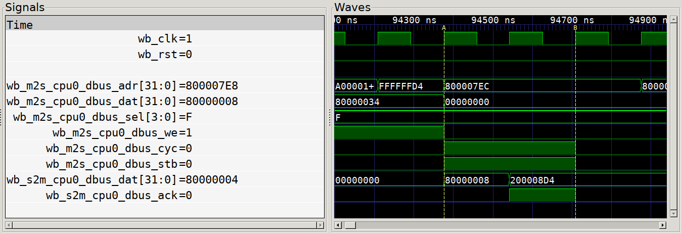
Classic Wishbone Transaction
There are other signals specified in the full Wishbone spec, such as errors, retry signals and tag data, but for many simple peripherals these signals are not implemented. For complex designs beyond the one shown here, or for further reference on the signals or formal properties of the bus, the full Wishbone Spec is an excellent reference. But for now, we know enough to be dangerous, and create some peripherals for our CPU.
The persistence of memory
To make a soft CPU useful, it needs to be fed instructions from somewhere. It’s also fairly common to want some amount of random access memory in excess of the built-in registers. To solve both of these problems, let’s write a quick memory module that can be accessed over the wishbone bus to provide either instructions or data to our CPU. Since both ROM and RAM are similar in behaviour here, we can reuse the same design for both. The implementation of a minimal working memory is something like the following (full code):
// Our main data storage. Yosys will replace this with an appropriate block ram
// resource.
parameter SIZE = 512; // In 32-bit words
reg [31:0] data [SIZE];

// Each data entry is 32 bits wide, so right shift the input address
// Sub-word indexing is achived through the byte select lines
localparam addr_width = $clog2(SIZE);
wire [addr_width-1:0] data_addr = i_wb_adr[addr_width+1:2];

integer i;
always @(posedge i_clk) begin
    if (i_reset) begin
        // Under reset we can't zero the memory contents, just ensure
        // that the wishbone bus returns to an idle state.
        o_wb_ack <= 1'b0;
    end else begin
        // Always ensure that our ack strobe defaults to low
        o_wb_ack <= 1'b0;

        // If we are being addressed, and this is not the cycle following an
        // ack, we need to perform a read/write
        if (i_wb_cyc & i_wb_stb & ~o_wb_ack) begin
            // We always read/write in the same cycle, so can
            // unconditionally set the ack here
            o_wb_ack <= 1'b1;

            // Always read the data at the given address to the output register
            // If this was a write operation, the data will simply be ignored
            o_wb_dat <= data[data_addr];

            // If this is a write, we need to do something a bit special here.
            // Since this memory needs to support non-32-bit operations, we
            // have to respect the byte select values. Handle this by looping
            // over each bit, and only writing the corresponding word if the
            // select bit is set.
            if (i_wb_we) begin
                for (i = 0; i < 4; i++) begin
                    if (i_wb_sel[i])
                        data[data_addr][i*8 +: 8] <= i_wb_dat[i*8 +: 8];
                end
            end
        end
    end
end
With this, we have something that can be read and written over wishbone (and we
can even add
some test cases
for it). This looks good for RAM, but for ROM we need a way to preload our
firmware into the memory. Verilog has system functions, $readmemb and
$readmemh that can load binary or hex data into a memory from a file. So,
let’s add another small feature so that we can tell our ROM memory to
initialize itself from the firmware hex we will generate later:
// If we have been given an initial file parameter, load that
parameter INITIAL_HEX = "";
initial begin
    if (INITIAL_HEX != "")
        $readmemh(INITIAL_HEX, data);
end
Connecting the blocks
Now that we have a CPU with a wisbone interface, and two wishbone peripherals, we just need to connect them all together. Writing all of the muxing and switching logic for this by hand would be extremely tedious, but luckily there exists an excellent tool, wb-intercon, that does the legwork for us. Given a YAML description of a bus (the masters, which slaves they connect to and what address they should see those slaves at) wb-intercon can generate all of the verilog necessary to mux and arbitrate the various signals.
So, to start off
with, let’s create a very simple wishbone layout that has two masters (our CPU
instruction and data bus ports) and two slaves, our ROM and RAM blocks. Note
that our ibus here only connects to the ROM, so executing from memory isn’t
allowed, but could of course be changed if you wanted to! We will arbitrarily
locate the rom at 0x20000000, and give it a max size of 4KiB. We will then
locate the RAM at 0x80000000, and only give ourselves 2KiB.
parameters:
  masters:
    cpu0_ibus:
      slaves: [cpu0_rom]

    cpu0_dbus:
      slaves: [cpu0_rom, cpu0_ram]

  slaves:
    cpu0_rom:
      offset: 0x20000000
      size:   0x1000

    cpu0_ram:
      offset: 0x80000000
      size:   0x800
If we run this through the wb-intercon generator, which in
the full project is done as
part of the CMake build,
we end up with two files - an implementation file,
which contains the modules responsible for the address decoding and signal
multiplexing, and a header file that contains all of the signal definitions for
our various bus participants. In order to connect up our modules, in our
top gateware file
we just need to include this header and then use the generated
wires to connect up our two wishbone RAM blocks, like so:
// Include the header that defines all the wishbone net names
`include "gen/wb_intercon.vh"

// CPU ROM.
// We initialize this directly from the hex file with our firmware in it
wb_ram #(
    .SIZE(1024), // In 32-bit words, so 4KiB
    .INITIAL_HEX("ice40_soc_fw_hex")
) cpu0_rom (
    .i_clk(wb_clk),
    .i_reset(reset),
    .i_wb_adr(wb_m2s_cpu0_rom_adr),
    [...]
    .o_wb_ack(wb_s2m_cpu0_rom_ack)
);

// CPU RAM
wb_ram #(
    .SIZE(512) // 2KiB
) cpu0_ram (
    .i_clk(wb_clk),
    .i_reset(reset),
    .i_wb_adr(wb_m2s_cpu0_ram_adr),
    [...]
    .o_wb_ack(wb_s2m_cpu0_ram_ack)
);
Once we similarly connect the iBusWishbone and dBusWishbone signals on
our CPU,
everything is in place for us to start writing some code to run on our new
system.
Baremetal RISC-V programming
Now that we have defined our hardware, we need to start defining our firmware. Since we do not have any operating system to handle hardware initialization and program startup for us, we must do it ourselves. This means getting hands on with the linker, the assembler and some low level features of the RISC-V architecture.
Defining our layout
At the end of our firmware compilation process, we need to end up with
a series of bytes
that represent the code our CPU should run and the values of any initialized
data. We can then load these bytes into the CPU, and should be up and running.
However to get here, we need to start by defining for the compiler how to
arrange that code, and at what addresses the running program can expect to
find things. In our earlier wishbone intercon YAML, we specified that the ROM
should appear at 0x20000000, and the RAM at 0x80000000.
Since we want to locate non-volatile
data in ROM and volatile data in RAM, we need to tell the linker where these two
memories exist, and what goes into each, so that it can generate correctly
addressed loads, stores and jumps.
The way to do this is in the linker script, the complete version of which is
here.
We define our memory regions (in this case we have just 2) with a MEMORY
directive, like so:
/* Define our main memory regions - we created two memory blocks, one to act as
 * RAM and one to contain our program (ROM). The address here should match the
 * address we gave the memories in our wishbone memory layout.
 */
MEMORY {
    ram (rwx)   :   ORIGIN = 0x80000000, LENGTH = 0x00000800
    rom (rx)    :   ORIGIN = 0x20000000, LENGTH = 0x00001000
}
This tells the linker that we have two regions where we can store data, and
how much data we can safely fit in each location. Both these values must match
the values used in the gatware, or there may be subtle problems later!
Now that we have defined the regions, we need to indicate what parts of our
program live in which section. We’ll start with the code itself, or the .text
section - this should contain
our initial startup code at the very beginning, followed by the rest of our
code, and any other read-only data:
.text : {
    /* Ensure that our reset vector code is at the very beginning of ROM,
     * where our CPU will start execution
     */
    *(.reset_vector*)
    /* General program code */
    *(.text*)
    /* Ensure that the next block is aligned to a 32-bit word boundary */
    . = ALIGN(4);
    /* Read-only data */
    *(.rodata*)
} >rom /* Locate this group inside the ROM memory */
Linker Relaxation
There are various other sections that must be located, all of which may be
found in the
full linkerscript,
but the other section I will flag here is one specific to the RISC-V
architecture - the .sdata (small data) and .sbss (small bss) sections.
The problem with a 32-bit ISA with 32-bit wide instructions is that it is
impossible for a single instruction to encode an offset that can address the
entire memory space - in reality, the immediate forms of memory load/store and
jump instructions can address only up to 21 bits from the current PC / other
base pointer. What this means is that operations referencing addresses over 2^21
bits away must be broken up into two operations - one to load an immediate into
a register, and another to perform the actual operation. This can be a
significant performance problem for some code, so RISC-V includes a feature
called Linker Relaxation. When the linker is assembling the final binary, it
will attempt to emit smaller jump/load instructions by addressing them relative
to a special register, the global pointer (gp) register. This register is
expected to be set to the address 0x800 bytes past the start of the small data
section, such that it can be used as a base for single-instruction addressing.
For a fuller explanation of linker relaxation, the SiFive blog has an excellent
post
here.
What makes this relevant to us is that we have some new sections in our linker
script, that we might miss if we were to assume the same layout as some other
embedded systems. In our linker, we need to be sure to actually include the
.sdata and .sbss sections (otherwise, statically initialized variables may
silently become zero-initialized!) and export the desired location of the global
pointer. For our data section, this results in a linker directive like the
following:
/* Our data segment is special in that it has both a location in rom (where
 * the data to be loaded into memory is stored) and in ram (where the data
 * must be copied to before main() is called).
 */
.data : {
    /* Export a symbol for the start of the data section */
    _data = .;
    /* Insert our actual data */
    *(.data*)
    . = ALIGN(4);
    /* Insert the small data section at the end, so that it is close to the
     * small bss section at the start of the next segment
     */
    __global_pointer$ = . + 0x800;
    *(.sdata*)
    . = ALIGN(4);
    /* And also make a note of where the section ends */
    _edata = .;
/* This section is special in having a Load Memory Address (LMA) that is
 * different from the Virtual Memory Address (VMA). When the program is
 * executing, it will expect the data in this section to be located at the
 * VMA (in this case, in RAM). But since we need this data to be
 * initialized, and RAM is volatile, it must have a different location for
 * the data to be loaded _from_, the LMA. In our case, the LMA is inside the
 * non-volatile ROM segment.
 */
} >ram AT >rom /* VMA in ram, LMA in rom */
Initialization
Now that we have our linker configured to locate our initialization code in the right place, and are exporting the addresses of important features such as the global pointer and initial stack pointer, we can start writing the lowest level code for our system. This startup code will initialize our stack, so that we can safely make function calls, the global pointer, so that linker-relaxed addressing works, and then call into our next section of initialization code:
# Since we need to ensure that this is the very first code the CPU runs at
# startup, we place it in a special reset vector section that we link before
# anything else in the .text region
.section .reset_vector

# In order to initialize the stack pointer, we need to know where in memory
# the stack begins. Our linker script will provide this symbol.
.global _stack

# Our main application entrypoint label
start:

# Initialize global pointer
# Need to set norelax here, otherwise the optimizer will convert this to
# mv gp, gp which wouldn't be very useful.
.option push
.option norelax
la gp, __global_pointer$
.option pop

# Load the address of the _stack label into the stack pointer
la sp, _stack

# Once the register file is initialized and the stack pointer is set, we can
# jump to our actual program entry point
call reset_handler

# If our reset handler ever returns, just keep the CPU in an infinite loop.
loop:
j loop
Once the assembly code above has initialized the state of the gp and sp
registers, we are able to safely start calling methods and executing code
beyond careful assembly, so for the next few initialization steps we jump to
the reset_handler method, which we will write in C:
// In our linker script, we defined these symbols at the start of the
// region in ROM where we need to copy initialized data from, and at the start
// and end of the data section that we need to copy that data to
extern unsigned _data_loadaddr, _data, _edata;

// Likewise, the locations of the preinit, init and fini arrays are generated
// by the linker, so we need to tell the compiler that they are defined
typedef void (*void_fun)(void);
extern void_fun __preinit_array_start, __preinit_array_end;
extern void_fun __init_array_start, __init_array_end;
extern void_fun __fini_array_start, __fini_array_end;

// In order for the reset_handler symbol to be usable by the assembly above, we
// need to protect it from the C++ name mangler.
// Likewise, we need to assert that there exists somewhere an application
// main() that we can invoke.
extern "C" {
int main(void);
void reset_handler(void);
}

void reset_handler(void) {
  // Load the initialized .data section into place
  volatile unsigned *src, *dest;
  for (src = &_data_loadaddr, dest = &_data; dest < &_edata; src++, dest++) {
    *dest = *src;
  }

  // Handle C++ constructors / anything with __attribute__(constructor)
  // These regions contain an array of function pointers, so we simply need to
  // iterate each and invoke them
  void_fun *fp;
  for (fp = &__preinit_array_start; fp < &__preinit_array_end; fp++) {
    (*fp)();
  }
  for (fp = &__init_array_start; fp < &__init_array_end; fp++) {
    (*fp)();
  }

  // At last, we can jump to our actual application level code
  main();

  // Should our application code ever exit (unusual in embedded), we may as
  // well run the desctructors properly
  for (fp = &__fini_array_start; fp < &__fini_array_end; fp++) {
    (*fp)();
  }
}
Memory-mapped IO
After building our way up from the bottom, we have finally arrived at the
application level. From here, we can implement int main() and proceed to
write firmware with impunity. But we didn’t come all this way just to run code
in isolation, we want our code to be able to reach out and interact with
the peripherals we build into our FPGA. So to that end, let’s take a look at
how memory mapped IO works from the firmware side.
We saw earlier that our CPU has two buses - an instruction bus and a data bus. When it needs to fetch instructions, the instruction bus reaches out over Wishbone and makes a read transaction at the relevant address. Similarly, if a load or store is executed, the data bus will generate a Wishbone transaction against the given location. But there is nothing that states that location has to be a memory - we are free to have those reads and writes be routed to any wishbone peripheral we desire. So let’s create a simple RGB LED controller that’s accessible over wishbone, and demonstrate how we can control and query it from our C code.
The core logic of our peripheral will look very similar to the memory we implemented a little while earlier, except that instead of a large block ram we will create some number of small registers to hold the data the peripheral needs to know. In this case, let’s say that our peripheral will be an 8-bit PWM generator with red, green and blue output channels. Since our registers can be up to 32 bits wide, we can pack the RGB component into one register and use a second to control the prescaler for our PWM generation. In verilog, this might look a little like this:
// PWM prescaler register
reg [31:0] pwm_prescaler;

// BGR output compare registers
reg [7:0] ocr_b;
reg [7:0] ocr_g;
reg [7:0] ocr_r;

// Wishbone register addresses
localparam
    wb_r_PWM_PRESCALER  = 1'b0,
    wb_r_BGR_DATA       = 1'b1,
    wb_r_MAX            = 1'b1;

// Since the incoming wishbone address from the CPU increments by 4 bytes, we
// need to right shift it by 2 to get our actual register index
localparam reg_sel_bits = $clog2(wb_r_MAX + 1);
wire [reg_sel_bits-1:0] register_index = i_wb_adr[reg_sel_bits+1:2];

always @(posedge i_clk) begin
    if (i_reset) begin
        o_wb_ack <= 0;
        pwm_prescaler <= 0;
    end else begin
        // As in our RAM before, we can default our ack strobe low
        o_wb_ack <= 1'b0;

        // If we are addressed by the cyc and stb lines, and are not in the ack
        // out cycle, we are in a transaction
        if (i_wb_cyc && i_wb_stb && !o_wb_ack) begin
            // Once again we do not have any delays, so we can ack
            // unconditionally
            o_wb_ack <= 1'b1;

            // Handle register reads
            // Note that our BGR data is 24 bits, so we pad it to 32
            case (register_index)
                wb_r_PWM_PRESCALER: o_wb_dat <= pwm_prescaler;
                wb_r_BGR_DATA:      o_wb_dat <= {8'd0, ocr_b, ocr_g, ocr_r};
            endcase

            // Handle register writes if the write enable flag is set
            if (i_wb_we) begin
                case (register_index)
                    wb_r_PWM_PRESCALER: pwm_prescaler <= i_wb_dat;
                    wb_r_BGR_DATA: begin
                        // For RGB writes, break out the data to the individual
                        // output compare registers
                        ocr_b <= i_wb_dat[23:16];
                        ocr_g <= i_wb_dat[15:8];
                        ocr_r <= i_wb_dat[7:0];
                    end
                endcase
            end
        end
    end
end
The full implementation of this module can be found
here.
Once we have granted this peripheral an entry in our wb intercon YAML and
connected it up in our
top module,
we can turn back to the firmware and take a
look at what’s necessary to interact with it. If we located our LED peripheral
at wishbone address 0x40002000, then in our C++ code if we read or write the
32-bit memory at that location, what we will actually be doing is reading or
writing the prescaler register of our LED block. It’s that easy! The only two
things we need to make sure we are clear about in our code is that
- This is a volatile memory address (the compiler may not assume that the last value written to it will be the next value read from it, or that writes may be dropped)
- We did not implement selective write logic for these registers - that is to say, if the CPU attempts to write these registers using 8 or 16 bit wide operations, it may corrupt the high bytes of the register! To prevent this, we must only use 32-bit wide accesses for these registers.
- The register indexing we used in our Verilog localparam is based on 32-bit
words, so the register with verilog index N is actually located in CPU memory
at
N * sizeof(uint32_t)past the start of the peripheral memory. We must therefore be careful when counting our register addresses.
To make following these rules simple, it helps to define some preprocessor macros as follow:
// Redefines an integer constant as a dereferenced pointer to a volatile 32-bit
// memory mapped IO register
#define MMIO32(ADDR) (*(volatile uint32_t *)(ADDR))

// Defines a register with 32-bit offset OFFSET
#define REG32(BASE, OFFSET) MMIO32(BASE + (OFFSET << 2))

// Now that we have our two macros above, we can quickly make some readable
// definitions for our LED driver
#define LED_BASE            0x40002000
#define LED_PWM_PRESCALER   REG32(LED_BASE, 0)
#define LED_BGR_DATA        REG32(LED_BASE, 1)
With only that, we can now read and write these registers from our code like
another variable. Let’s finally implement a main() and cycle some colours on
our LED:
#define CPU_CLK_HZ 42'000'000

uint32_t led_states[] = {
    0x000080,
    0x008000,
    0x800000,
    0x0000FF,
    0x00FF00,
    0xFF0000,
};

void delay(uint32_t cycles ) [
    while (cycles--){
        asm volatile ("nop");
    }
}

int main(void) {
    // Initialize our PWM prescaler to generate a 1kHz carrier with 8 bit pwm
    LED_PWM_PRESCALER = (CPU_CLK_HZ / 256 / 1'000) - 1;

    // Iterate through each of our LED states, with a delay so that we can
    // actually see what is going on
    for (int i = 0; i < sizeof(led_states) / sizeof(uint32_t); i++) {
        LED_BGR_DATA = led_states[i];
        delay(CPU_CLK_HZ / 2); // Very approximately one second
    }
}
Interrupts
While our above demo is very blinky, it’s not particularly elegant - our delay loop just burns CPU cycles, and it would be hard to do cycle counting if we were trying to achieve a number of timed tasks at the same time. Instead it would be a lot more useful if we could somehow keep track of the current time, and only advance the LED state after a given number of milliseconds.
Luckily, building a timer is very much within our reach - with enough gates we can build anything! But how do we tie the timer back into our CPU without just busy waiting on a timer register instead of a NOP loop? One solution to this problem is interrupts. If we build a timer module and connect it to one of the interrupt lines on our CPU, our CPU can then jump to an interrupt handler that either updates our LEDs directly, or simply updates a counter we can reference from our main loop.
Let’s start with the verilog timer module. We don’t need anything too fancy, but we do want to be able to at least configure the prescaler for the counter on the fly, so that we can adjust the interrupt rate in our firmware. We also need to be able to clear the interrupt signal from the timer, so it’s back to the Wishbone peripheral structure we are getting increasingly familiar with.
The first part of a timer is simple: we need to be able to count. In this case, we count down from our configured prescaler to zero, then reload the prescaler and start all over again, something like this:
// Prescaler value. Reloaded onto the downcounter on update.
reg [31:0] prescaler = 32'hFFFF_FFFF;;

// Downcounter. Trigger output is latched high when this hits zero.
reg [31:0] downcounter = 32'hFFFF_FFFF;;

// Trigger output signal
reg timer_trigger = 0;

// Downcount until the counter reaches zero, then reload the prescaler and
// start counting down again
always @(posedge i_clk) begin
    if (downcounter > 0) begin
        downcounter <= downcounter - 1;
    end else begin
        downcounter <= prescaler;
        timer_trigger <= 1'b1;
    end
end
Now that we have that, we need to add enough wishbone logic to allow for setting the prescaler, and for clearing the timer trigger when it is set. Since interrupts on the CPU are level-triggered, if we don’t clear the interrupt source, the CPU will end up returning from and re-entering the timer interrupt forever!
// Wishbone register addresses
// Each register is 32 bits wide
localparam
    wb_r_PRESCALER  = 1'b0,
    wb_r_FLAGS      = 1'b1,
    wb_r_MAX        = 1'b1;

// Bit indices for the flags register
localparam
    wb_r_FLAGS__TRIGGER = 0;

// Since the incoming wishbone address from the CPU increments by 4 bytes, we
// need to right shift it by 2 to get our actual register index
localparam reg_sel_bits = $clog2(wb_r_MAX + 1);
wire [reg_sel_bits-1:0] register_index = i_wb_adr[reg_sel_bits+1:2];

always @(posedge i_clk) begin
    // Default the ack signal to a zero state.
    // Later writes to this register will take precedence if we are actually
    // performing a wishbone transaction
    o_wb_ack <= 1'b0;

    // If the cycle and strobe inputs are high, and this is not the cycle after
    // a previous transaction, we are servicing an actual wishbone request
    if (i_wb_cyc && i_wb_stb && !o_wb_ack) begin
        // None of our operations take more than one cycle, so we can always
        // unconditionally ack the request
        o_wb_ack <= 1'b1;

        // To handle writing the prescaler / clearing flags, we need to check
        // if this is a write request
        if (i_wb_we) begin
            // If it is, use the address bits to select the appropriate
            // register to work with
            case (register_index)
                wb_r_PRESCALER: begin
                    // Load the new prescaler, and also reset the downcounter
                    // If we don't reset the downcounter, we run the risk that
                    // the previously loaded value was extremely large and will
                    // delay 'proper' operation at the new prescaler rate
                    prescaler <= i_wb_dat;
                    downcounter <= i_wb_dat;
                end
                wb_r_FLAGS: begin
                    // If this is a write to the flags register, we want to
                    // check which flags are being cleared.
                    // If the trigger bit is written, we clear the trig state.
                    if (i_wb_dat[wb_r_FLAGS__TRIGGER])
                        timer_trigger <= 1'b0;
                end
            endcase
        end
    end
end
Note - in the two preceding snippets, the timer_trigger register is written
to from two different always blocks - this is not valid verilog! If you are
going to copy parts of this module, please do so from the
full source code.
Now that we have a timer implementation, the only remaining change to make in
gateware is connect up the timer trigger output wire to the timer interrupt
input on our CPU, and to connect the timer to the wishbone bus wires we
generated with our wb_intercon file.
// Timer for generating the timer interrupt
wire timer_interrupt;
timer_wb #(
    .DEFAULT_PRESCALER(`CLOCK_HZ / 1000 - 1)
) timer0 (
    .i_clk(wb_clk),
    .i_reset(reset),
    .o_timer_trigger(timer_interrupt),
    [...]
);

// CPU
VexRiscv cpu0 (
    [...]
    // Interrupt sources
    .timerInterrupt(timer_interrupt),
    .externalInterrupt(1'b0),
    .softwareInterrupt(1'b0),
    [...]
);
With that hooked up, our gateware is good to go! Let’s take a quick look at our simulation and see that interrupt in action:
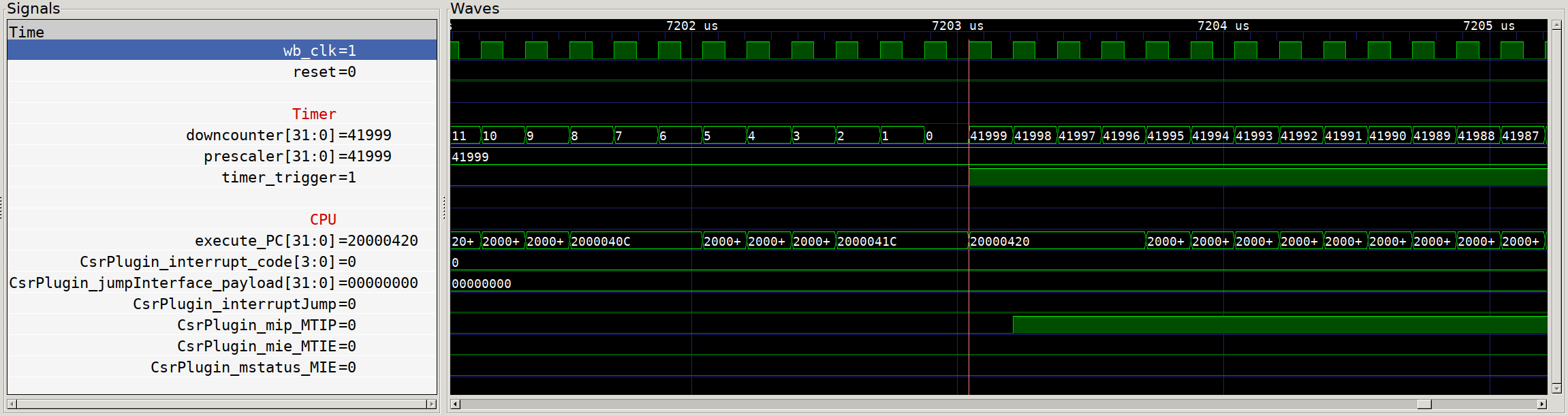
Timer interrupt execution?
Except… we see nothing! Our timer counts down and sets the trigger output, but our CPU ticks along as though nothing has happened. What gives! The clue here is the additional signals on screen - the default value of the Configuration and Status Registers (CSRs) that relate to interrupts have all interrupts disabled by default. So even though we see that the Machine Timer Interrupt Pending (MTIP) flag is set, nothing happens. So we need to switch over to our firmware and make sure that we configure the CPU properly to handle our interrupts.
The first register we need to configure is the Machine Trap-Vector Base-Address
register, or mtvec. This register is used to store the
memory address that the CPU will jump to in the event of an interrupt.
Since the address must be 32-bit aligned, the low 2 bits are used to control
the interrupt mode, where a value of 0x0 is direct (all exceptions jump to
the mtvec address) and a value of 0x1 is vectored (interrupts set the program
counter to (mtvec + (4 * exception_code)).
In vector mode, mtvec must therefore be the start of a series of jump
statements to specific exception handlers, instead of the entry point to a
single exception handler. For simplicity we will use the non-vectored version
and work out how to handle the interrupt in software. But before we can set the
mtvec address at all, we need some sort of interrupt handler routine to point
it to, so let’s create one now.
// We need to decorate this function with __attribute__((interrupt)) so that
// the compiler knows to save/restore all register state, as well as to
// re-enable interrupts on return with the mret instruction.
void __attribute__((interrupt)) interrupt_handler(void) {
    // When an interrupt occurs, the mcause register contains the interrupt type
    uint32_t mcause;
    asm volatile("csrr, %0" : "=r"(mcause));

    // The top bit of mcause is the sync vs async exception bit, we don't
    // handle that here so mask it off
    mcause &= 0x7FFFFFFF;

    // If the cause is some number out of range of our handler table, we have
    // no way to handle this interrupt! Block forever.
    if (mcause >= (sizeof(vector_table) / sizeof(isr_vector))) {
        while (true) {}
    }

    // Otherwise, we can jump to the handler listed in our vector table.
    // Since we took care to order our struct to match the interrupt IDs, we can
    // reinterpret it as an array for easy indexing based on mcause
    ((isr_vector *)&vector_table)[mcause]();
}
Now you’ll note that in the code above we made some reference to a vector table - since we are decoding the interrupt cause ourselves, we need some structure that contains pointers to the handlers for each of our interrupts. To keep things well named, we use a struct that has the same layout as the interrupt numbering scheme used by RISC-V, like so:
// Create a type alias for our exception handlers, which are void functions
typedef void (*isr_vector)(void);

// The basic interrupts for RISC-V are the software, timer and external
// interrupts, each of which is specified for the user, supervisor and machine
// privilege levels.
struct {
    // Software interrupt
    isr_vector software_user_isr = &blocking_handler,
    isr_vector software_supervisor_isr = &blocking_handler,
    isr_vector software__reserved = &blocking_handler,
    isr_vector software_machine_isr = &blocking_handler,
    // Timer interrupt
    isr_vector timer_user_isr = &blocking_handler,
    isr_vector timer_supervisor_isr = &blocking_handler,
    isr_vector timer__reserved = &blocking_handler,
    isr_vector timer_machine_isr = &timer_interrupt,
    // External interrupt
    isr_vector external_user_isr = &blocking_handler,
    isr_vector external_supervisor_isr = &blocking_handler,
    isr_vector external__reserved = &blocking_handler,
    isr_vector external_machine_isr = &blocking_handler,
} vector_table;
This struct, when compiled, turns into an array of function pointers that we
can index directly with mcause. For interrupts that we don’t explicitly
handle yet, we point to a simple blocking handler that loops forever, hanging
the CPU so that we can detect something has gone wrong.
The one interrupt that we do actually want to handle properly right now, the
timer interrupt, is pointer to a timer_interrupt function, which we will
define like so:
// Our counter is modified from an interrupt context and read from a
// non-iterrupt context, so we need to mark it volatile to ensure accesses hit
// main memory each time
volatile uint32_t time_ms = 0;
void timer_interrupt(void) {
    // Increment the millisecond counter
    time_ms++;

    // We need to also clear the source of the interrupt, otherwise when we
    // return from interrupt it will just fire again right away.
    TIMER_FLAGS |= TIMER_FLAGS__PENDING;
}
Alright, we now have all the handler code that we should need once our interrupt actually fires. However, we still have yet to actually enable interrupts or tell the CPU where exactly to go when an interrupt is triggered. In order to do this, let’s add some code early in our firmware initialization that sets the relevant CSRs:
// Firstly, let's update the machine interrupt vector CSR with the address of
// our base interrupt handler.
// Since our address is 32-bit aligned, we are in non-vectored mode by default
asm volatile("csrw mtvec, %0" ::"r"(&interrupt_handler));

// We now want to enable the machine timer interrupt. To do this, we need to
// set bit 7 in the Machine Interrupt Enable (mie) register
// We use the assembler shorthand CSR Set bit instruction here for convenience
// Note that the literal 1<<7 is here marked as a register operand - the CSRS
// instruction only supports 5-bit immediates
asm volatile("csrs mie, %0" ::"r"(1<<7));

// We then need to enable machine interrupts globally, by setting bit 3 in the
// Machine Status Register (mstatus).
// Here, 1<<3 fits in the immediate form of the instruction ("i")
asm volatile("csrs mie, %0" ::"i"(1<<3));
Finally, we should have completed all the necessary legwork to get timer interrupts running on our CPU. To verify, let’s take another look at our simulated system:
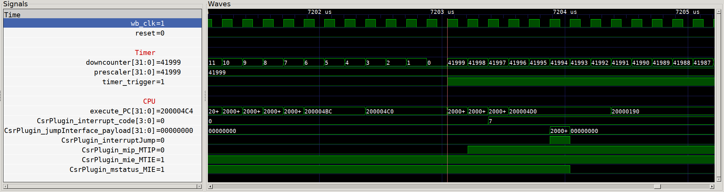
Timer interrupt execution with MTIE and MIE enabled
Much better! We can see that the MTIE and MIE bits are now set, and that we
have a clear cycle by cycle progression of our timer output signal going high,
being registered in the CPU as a pending timer interrupt (MTIP), the
corresponding interrupt code (7) being loaded in mcause, and finally the
CSR-triggered jump to our interrupt handler at 0x200000190. If we were to
zoom out on the scope above, we would later see the timer trigger be cleared by
the write in our timer interrupt handler to the timer flags register, the
deassertion of MTIP and the return to normal code execution.
If we build and deploy this with a couple of tweaks to our colour generation (see full code here) we should end up with a lovely changing colour cycle running on our dev board:
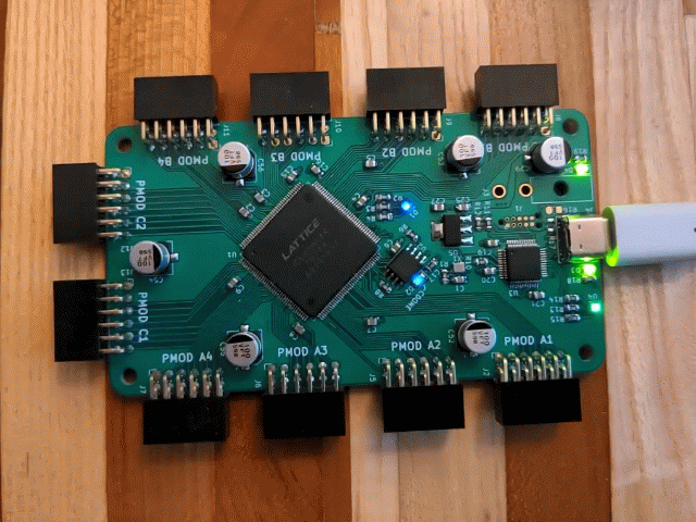
Interrupt-powered RGB cycling
The full source code for all gateware, firmware, tests and simulations used in this post can be found on Github here. The repo also contains some code and peripherals that we did not cover here, such as a buffered UART peripheral.
Design files and assembly instructions for the FPGA board shown in the image above can be found in this previous post.