FPGAs 1: Running on Hardware
Sun, Mar 29, 2020 Companion code for this post available on GithubAfter going over the basic idea of what an FPGA is and running some simulations in the last post, the next logical step is to take things from the computer and into the real world. To that end, this post will attempt to cover the entire journey from PCB design to running gateware on an assembled board in such a way as to make it accessible to those new to FPGA development. Some implementation details have had to be left out for brevity, but every piece of CAD, firmware, and gateware referenced in this post can be found in this git repo for those that want to read deeper.
The Hardware
The hardware designed to accompany this post is a breakout board consisting of a Lattice ICE40 series HX4K FPGA, one of the few FPGAs that comes in an easy(er) to solder quad flat leaded package. The FPGA IO are broken out to 10 standard PMOD connectors, for a total of 80 external IO lines. There is also an ARM based STM32F070CBT6 microcontroller, with two hardware SPIs connected across to the FPGA (one shared with the flash), one hardware UART connected to the FPGA and a USB interface for communicating with a host computer. Full hardware design files can be found in the hardware/ folder. Feel free to use this design as a reference for further work, but if you do, bear in mind a couple of design points.
The first is that (most) FPGAs are volatile - they do not maintain their configuration if they are power cycled, and so every time they turn on they must be reconfigured before they will operate. This can be done automatically by the FPGA acting as a SPI master to read from a flash device, by having the FPGA acting as a SPI slave and receiving the bitstream data from a microcontroller or other device, or over JTAG.
To make turning on our FPGA board as simple as possible, we will include a flash chip connected to the FPGA to provide storage for the bitstream. However, we also need some way to program the bitstream onto the flash chip. One approach is to place an FTDI device such as the FT2232 on the board, which allows reading/writing the flash using MPSSE instructions. However, these chips are a bit expensive (Over $6 in quantity 1), and the functions they are performing aren’t overly complex. This is why for this design we instead use a cheap ARM based microcontroller with USB support to perform flash operations. In addition, the microcontroller code can be extended with application code to extend the functionality of the system.
The second thing to take note of is that FPGAs generally have a number
of different voltage rails that must be supplied. The FPGA
core generally runs at a fairly low voltage - here 1.2V. However, FPGAs have
separate supply pins for the IO voltage level (VCCIO), which can be
set differently per IO bank if you need to interface with multiple devices at
different voltage levels. In our case, we’re going to use 3.3V as our IO
voltage, since it is fairly widely compatible and is also the voltage for our
microcontroller.
Third, one of the biggest advantages of routing FPGA designs is the lack of constraints around pinout - since any IO pin can be any function, we are fairly free to shuffle our connections between FPGA and PMOD to achieve more direct routing. However, there are some small exceptions - certain pins on the device will be listed as being directly connected to ‘global buffers’, or other special purpose routing constructs that provide high signal fanout / low timing skew within the device itself. If you have any signals coming into the FPGA that are likely to be used in many places (e.g. a clock), it is generally advantageous to connect those signals to a hardware pin that has a dedicated connection to one of the high-fanout internal buffers.
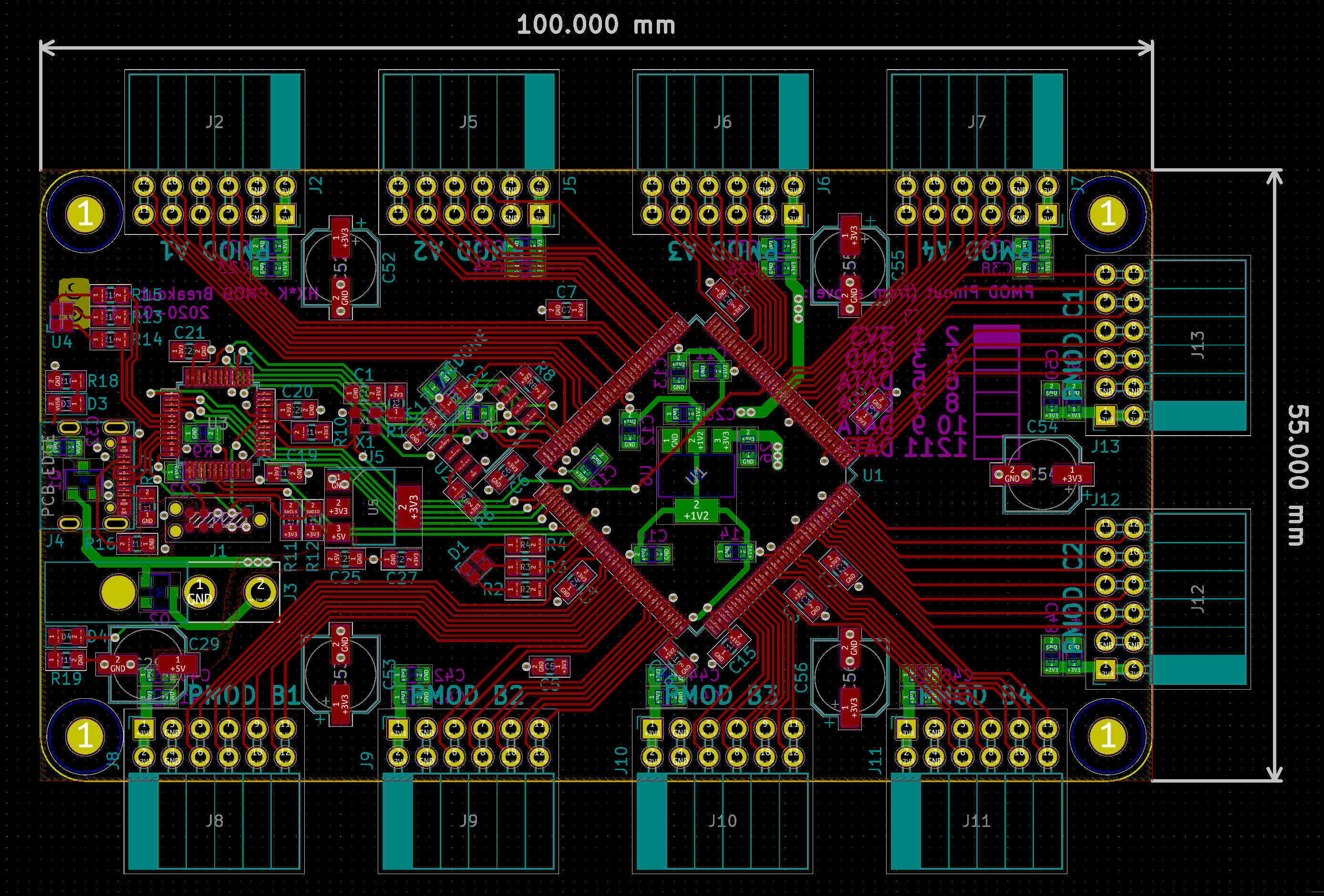
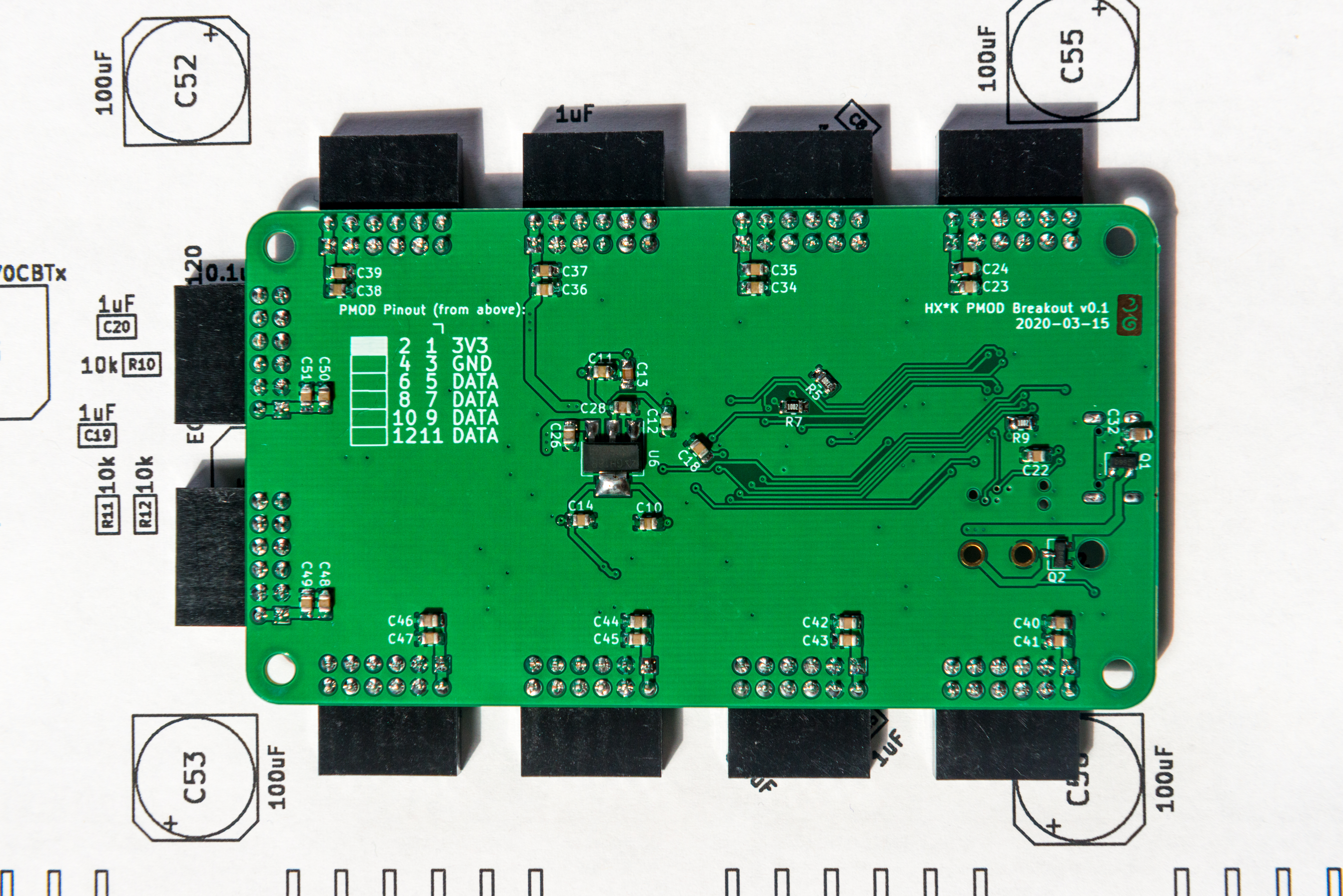
Finished design. 2 Layers.
Building Your Owm
If you want to build your own copy of this breakout board, you will first need to acquire some blank PCBs. If you have done this before, you can clone the repo containing all of the design files (gerbers are in hardware/gerber/) and ship the Gerbers to your preferred PCB manufacturer. Alternately, or for convenience, you can order this design directly from PCBWay, a budget PCB house with respectable quality and turnaround time.
While you wait for your boards, you may also need to order components. The KiCad design files are fully specified with the manufacturer and DigiKey part numbers for all components involved. Also included in the hardware/ folder is a DigiKey BOM (digikey_bom.csv), which can be uploaded to the DigiKey BOM Tool and used to immediately add the necessary components to an order. Note that the BOM item quantity is for precisely one unit - I would recommend going through and adding whatever fudge factor you feel is reasonable to cheaper passives and other parts you want some margin for error with.
At time of writing, the total cost of the BOM for no more than one board is $37.60. If you intend to make more than one, the unit price will go somewhat as you hit the price breaks.
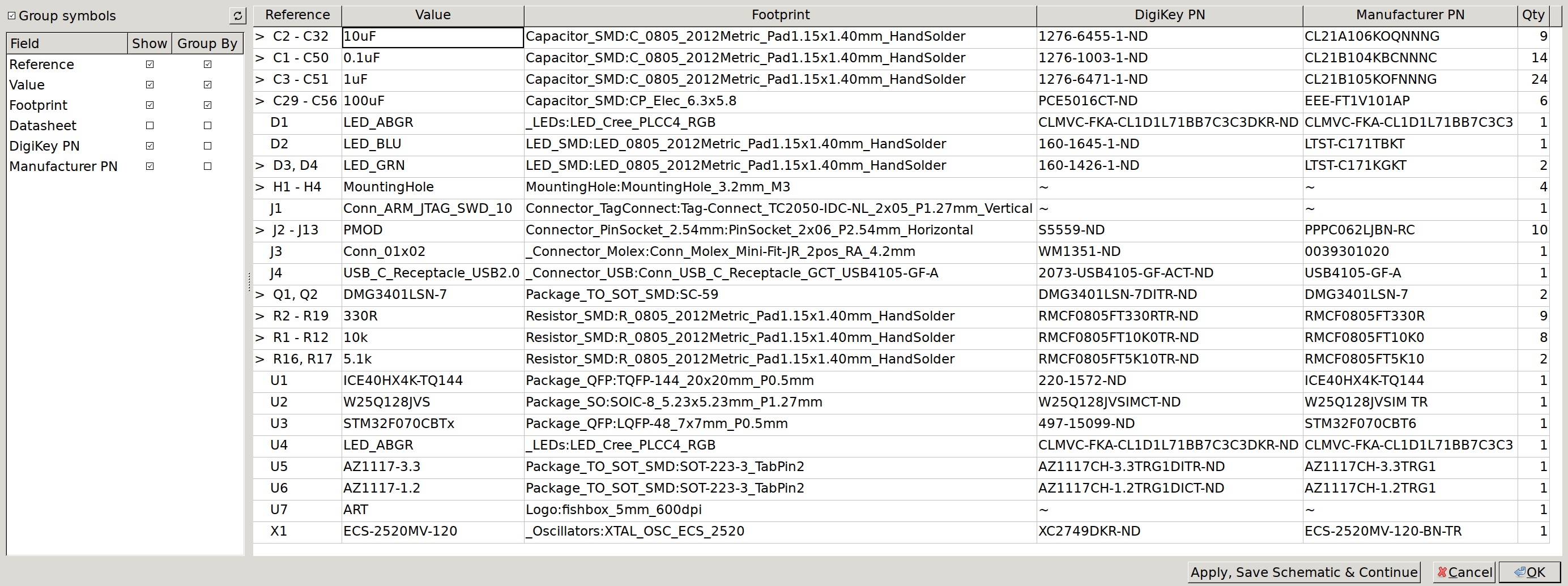
Overview of BOM in KiCad Table Editor
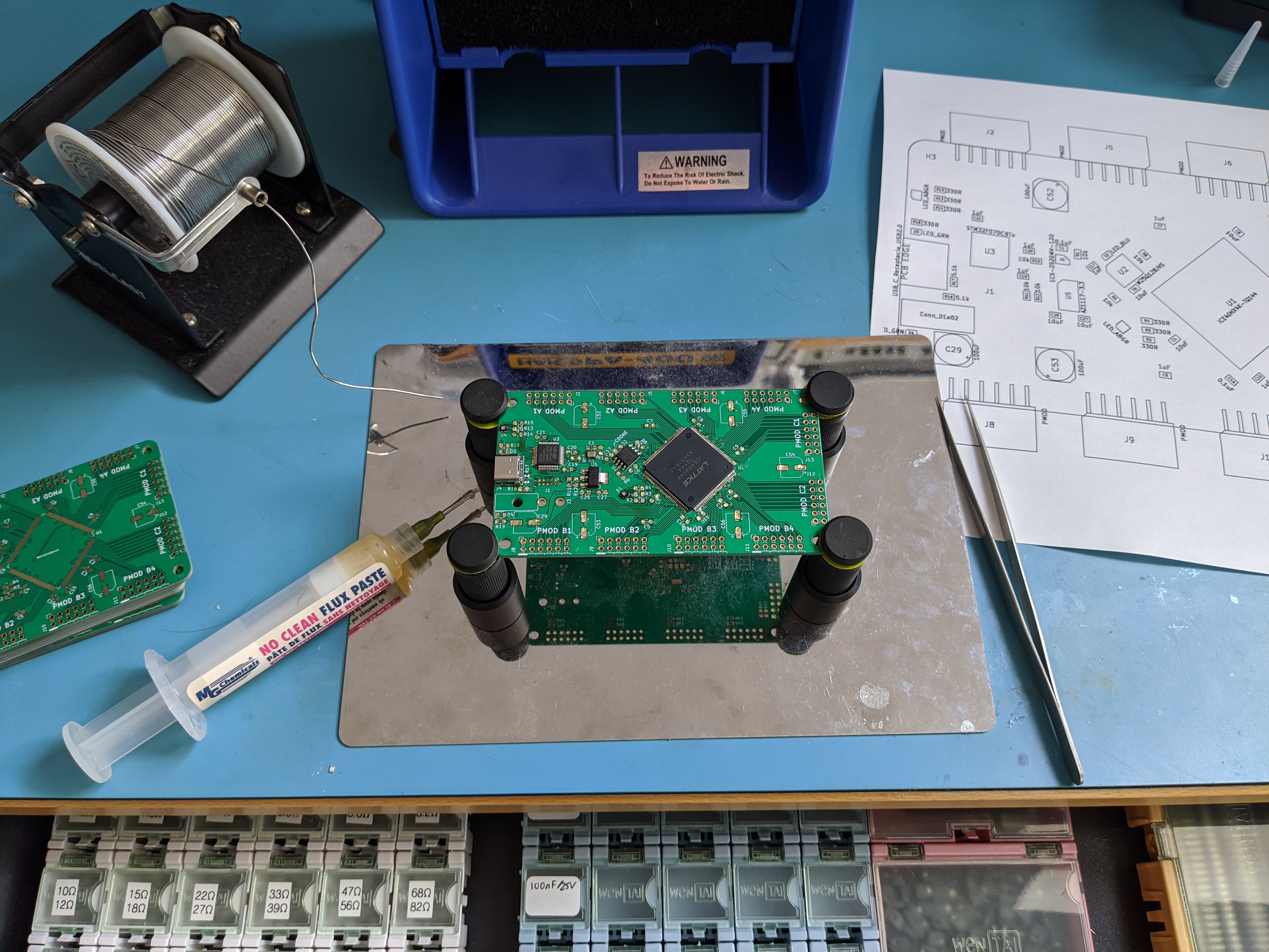
Once you have the parts and boards, there are a couple other prerequisites for assembly -
- Soldering iron (TS-100 or TS-80 would be fine for this)
- Flux (Massively simplifies the soldering of the QFP packages)
- Fine tweezers (I recommend Rhino SW-11 or comparable)
- [Optional] Board holder. I find PCBite setup to be extremely worth it.
- [Optional] Hot air rework station. The ‘858D’ hot air station is available from many resellers at reasonably prices, and is more than adequate.
One of the design goals for this board was for it to be feasible to assemble by hand, using only a soldering iron. To that end, all of the critical components are leaded packages, and there are no passives smaller than 0805. For some components (USB type-C connector J4, 12MHz oscillator X1 and RGB LEDs D1 and U4), a hot air gun may be advantageous, but it is possible to get away without one.
Component placement for assembly
If like me you use a fair amount of flux during assembly, I would recommend washing the PCB afterwards using first some flux cleaner and an ESD toothbrush, followed by a rinse in some 99% isopropyl alcohol. You can then leave the board to air dry, or apply (gentle!) heat with the hot air gun to evaporate any remaining isopropyl.
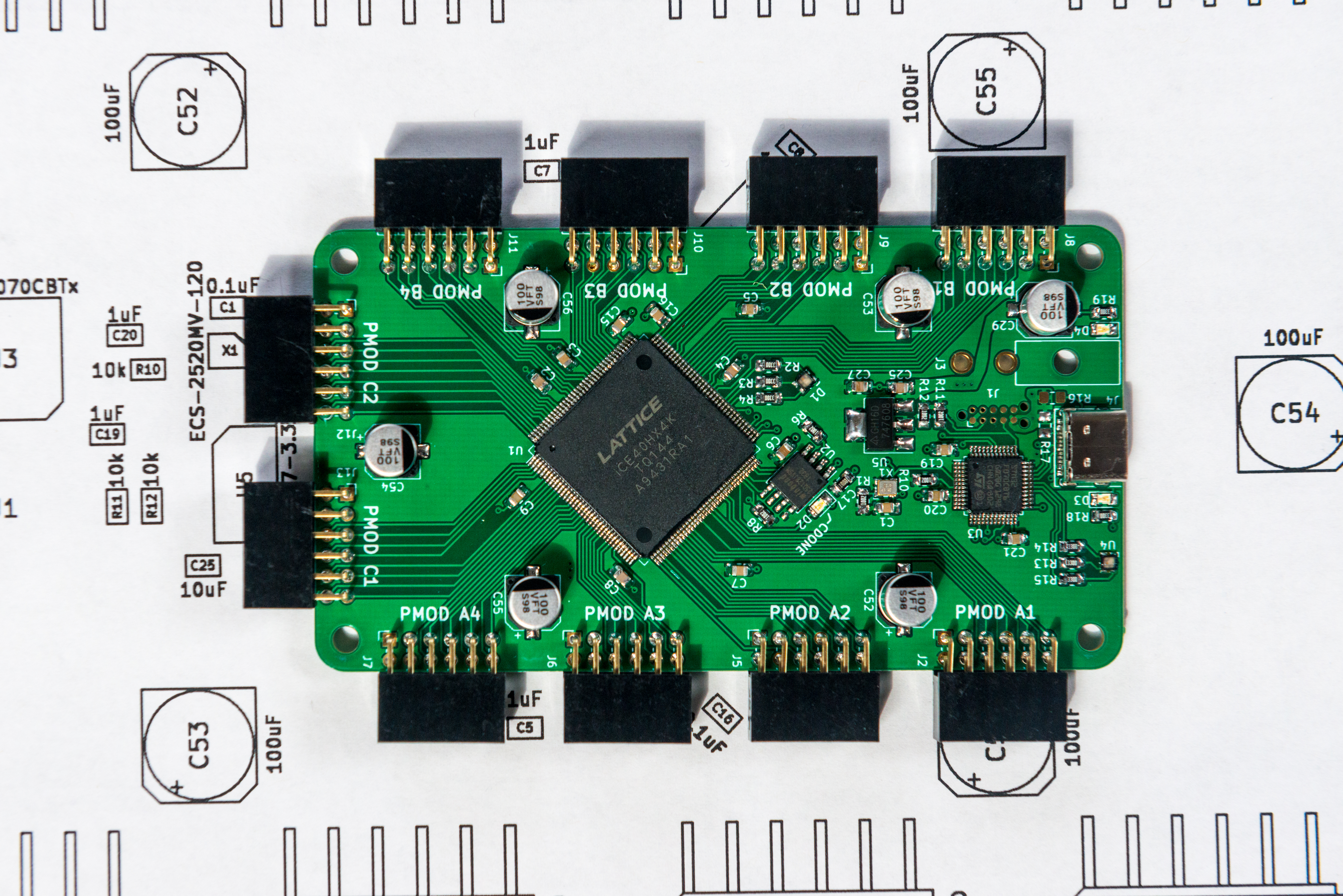
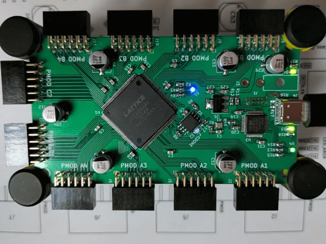
Finished Assembly (Front)
Finished Assembly (Back)
Interfacing to the Computer
Now that we have our board assembled, we need to be able to write bitstreams to it, otherwise it isn’t very useful. In order to do this, we’re going to need to write some firmware for the onboard microcontroller that will allow us to perform a programming flow along the lines of
- Put the FPGA into reset
- Erase and reprogram the flash
- Take the FPGA out of reset
- Act as an intermediary if we implement a UART on the FPGA
For that we are going to use a STM32F0 series part and the open source libopencm3 HAL. For more information on getting started with that programming environment, I would recommend reading through this series of posts.
The core of our firmware is going to be listening for incoming packets over
one USB endpoint, figuring out what operation is intended, and then potentially
responding back to the computer. The full implementation can be seen in
usb_protocol.cpp,
but that basic idea is that we use the first byte of any incoming USB packet to
determine the command. Since we have a bounded number of commands, we have a
lookup table that maps the command code to an appropriate handler function. For
example, here is the handler for the UsbProto::Opcode::FPGA_RESET_ASSERT
command, which puts the FPGA into reset in anticipation of programming:
void UsbProto::handle_fpga_reset_assert(const uint8_t *buf, int len) {
  // In order to program the flash, we want to make sure that we aren't in
  // contention with the FPGA for control over the SPI lines. The first thing
  // to do here is therefore to pull the NRESET line of the FPGA low
  FPGA::assert_reset();
  // Once the FPGA is no longer driving any signals, we can enable the hardware
  // SPI on our microcontroller, taking control of the bus.
  SPI::init();
  // Once the spi is ready, we send a few initialization commands to the flash
  // chip to ensure it is ready to perform reads / writes.
  Flash::init();
  Flash::reset();
  Flash::wakeup();
}
The vast majority of this code should apply to other boards designed around a microcontroller programming interface in this way, so in an attempt to make this firmware easy to port to your own projects, all pin configuration data is contained in a single header file, include/config.hpp, so that it can be adapted for slightly different implementations.
To get the firmware uploaded, you will need some sort of SWD adapter (my go-to being the BlackMagic Debug Probe), and a TagConnect 2050 cable in order to connect to the programming pads. To build:
# Install ARM toolchain
sudo apt install gcc-arm-none-eabi gdb-arm-none-eabi binutils-arm-none-eabi
# Clone & build the firmware repo
git clone git@github.com:rschlaikjer/hx4k-pmod.git
cd hx4k-pmod
git submodule init
git submodule update
# Build
mkdir programmer_firmware/build
cd programmer_firmware/build
cmake ../
make -j$(nproc)
Once the binary is built, if you are using the black magic probe (and it is
connected as /dev/ttyACM0), you can flash the device by first connecting it
to power through either the USB header or auxiliary power jack, and then
building using the CMake target
fpga_programmer_flash. You should see output similar to the following:
ross@mjolnir:/h/r/P/G/f/p/build$ make fpga_programmer_flash
[ 44%] Built target libopencm3
[100%] Built target fpga_programmer_elf
Black Magic Probe (Firmware v1.6.1-311-gfbf1963) (Hardware Version 3)

Available Targets:
No. Att Driver
 1      STM32F07 M0
event_loop () at /home/ross/Programming/Github/fpga-swe-1/programmer_firmware/src/main.cpp:87
Loading section .text, size 0x29e4 lma 0x8000000
Loading section .init_array, size 0x8 lma 0x80029e4
Loading section .data, size 0x14 lma 0x80029ec
Start address 0x8001e84, load size 10752
Transfer rate: 18 KB/sec, 768 bytes/write.
Section .text, range 0x8000000 -- 0x80029e4: matched.
Section .init_array, range 0x80029e4 -- 0x80029ec: matched.
Section .data, range 0x80029ec -- 0x8002a00: matched.
Kill the program being debugged? (y or n) [answered Y; input not from terminal]
[100%] Built target fpga_programmer_flash
You should then see the board show up as a USB device, with the default VID:PID set to a generic test PID:
ross@mjolnir:/h/r/P/G/f/p/build$ lsusb -d 1209:0001
Bus 001 Device 106: ID 1209:0001 Generic pid.codes Test PID
However, this firmware is only one half of the programming flow - we also need a program to run on the host computer and send the necessary control/data packets to the device. To that end, I have created a tool to Find and Flash FPGAs called faff, which speaks the simple USB protocol we’ve defined in the firmware. The implementation of the host side of the USB commands can be seen in src/usb_protocol.cpp, and follows the same naming as used in the firmware, Requests are by and large fairly straightforward - for example, here is the implementation for writing data to flash:
void Session::cmd_flash_write(uint32_t addr, const uint8_t *data,
                              uint8_t size) {
  // Our packet structure must contain
  // - One byte operation (FLASH_WRITE)
  // - Four byte write offset (MSB first)
  // - One byte indicating how many data bytes follow
  // - N data bytes to be written to flash
  uint8_t cmd_out[size + 6] = {
      static_cast<uint8_t>(Opcode::FLASH_WRITE),
      ((uint8_t)(addr >> 24)),
      ((uint8_t)(addr >> 16)),
      ((uint8_t)(addr >> 8)),
      ((uint8_t)(addr >> 0)),
      size,
  };
  // Copy the data to be sent into our output packet buffer
  memcpy(&cmd_out[6], data, size);

  // Ask libusb to send this packet to the device.
  int transferred = 0;
  int ret =
      libusb_bulk_transfer(_usb_handle, _args._usb_endpoint_tx, cmd_out,
                           sizeof(cmd_out), &transferred, libusb_timeout_ms);

  // If libusb failed to write out this packet, we will abort here.
  assert_libusb_ok(ret, "Failed to initiate flash write");
}
To build this tool, make sure you have libusb’s development headers installed, and then build it using CMake:
# Install dependencies
sudo apt install -y build-essential cmake libusb-dev
# Clone the repo
git clone git@github.com:rschlaikjer/faff.git
# Build as a normal CMake project
mkdir faff/build
cd faff/build
cmake ../
make -j$(nproc)
# Optionally
sudo cp faff /usr/local/bin
Once faff is installed and in your $PATH, we can use it to list connected
targets using the -e|--enumerate option, and then load a file using -f:
ross@mjolnir:/h/r/P/G/f/build$ ./faff -e
Searching for devices with VID:PID 1209:0001
[0] Serial: 004700254753511120303234
Found 1 devices

ross@mjolnir:/h/r/P/G/f/build$ ./faff --usb-serial 004700254753511120303234 -f top.bin
Claimed device 1209:0001 with serial 004700254753511120303234
Flash chip mfgr: 0xef, Device ID: 0x17 Unique ID: 0xe4682c404b163333
Programming block 0x00020fa0 / 0x00020fbc
Reading block 0x00020fa0 / 0x00020fbc
faff has a couple more options, which can be found by running it with the
--help flag. But for now, being able to detect and write files to the flash
is all we need.
Synthesizing Gateware
Finally, we have gotten to the point where we can actually start on the FPGA part of this FPGA breakout board. If you haven’t already, download and install the open source FPGA toolchain consisting of yosys, icestorm (since this is an ice40 part) and nextpnr. Instructions for all of them are on their respective homepages.
The first thing we need to do when bringing up an FPGA board is define the pin mapping. For this, we need a ‘Physical Constraint File’ (pcf). This is something you generally only need to do once per hardware design, and will then be applicable for any applications running on that hardware. The syntax is fairly straightforward (full file for this board can be found here), and assigns a name to a given FPGA pin (by number, for QFx packages, or by ball, for BGA packages):
# Input 12MHz oscillator is connected to physical pin number 21
set_io -nowarn CLK_12MHZ 21

# RGB led has three connections, on FPGA pin numbers 83-85
# Also, note that these LEDs are active LOW!
set_io -nowarn LED_R        84
set_io -nowarn LED_G        85
set_io -nowarn LED_B        83
When we then create our top-level Verilog module, we are able to use any signal defined in the PCF file as a module connection, like so:
`default_nettype none
`define CLK_HZ 12_000_000
module top(
        // Input clock
        input wire CLK_12MHZ,

        // RGB LEDs
        output wire LED_R,
        output wire LED_G,
        output wire LED_B
    );

    // To blink the LEDs at a human scale, let's have a counter that
    // rolls over at approximately 4Hz. Note that this is not a proper
    // prescaler - we're just getting a power of two in the right ballpark
    localparam PRESCALER_4HZ = (`CLK_HZ / 4) - 1;
    reg [$clog2(PRESCALER_4HZ):0] counter;

    // And assign the LED outputs to be the higher (slower) bits of
    // that counter
    assign LED_R = counter[$clog2(PRESCALER_4HZ)];
    assign LED_G = counter[$clog2(PRESCALER_4HZ)-1];
    assign LED_B = counter[$clog2(PRESCALER_4HZ)-2];

    // At every rising clock edge, increment that counter by one
    always @(posedge CLK_12MHZ) begin
        counter <= counter + 1;

endmodule
If you cd to the
gateware/
directory in the repo that accompanies this project and run make, you
should see it synthesize, place and pack a demo bitstream that will blink some
LEDs as a sign of life. If all goes well, you should see this output:
icepack top.asc top.bin
// Reading input .asc file..
// Reading 8k chipdb file..
// Creating timing netlist..
// Timing estimate: 5.01 ns (199.63 MHz)
// Checking 20.83 ns (48.00 MHz) clock constraint: PASSED.
Now that you have a top.bin file, you can use faff to load it onto the
board using the make prog target (assuming faff is in your $PATH):
ross@mjolnir:/h/r/P/G/f/gateware$ make prog
faff -f top.bin
Claimed device 1209:0001 with serial 004700254753511120303234
Flash chip mfgr: 0xef, Device ID: 0x17 Unique ID: 0xe4682c404b163333
Programming block 0x00020fa0 / 0x00020fbc
Reading block 0x00020fa0 / 0x00020fbc
If all goes well, you should be greeted by a green light on the MCU status LED, and a multicoloured blink pattern from the FPGA:
Demo gateware blinking
The demo verilog provided also instructs the FPGA to echo back any UART signals
it receives. To verify that this is working properly, connect to the serial
port of the board (here ttyACM2) and try typing some characters. You should
see them show up in the serial console as they are received, echoed by the FPGA
and sent back over USB. You can connect using screen as a serial monitor
with the command screen /dev/ttyACM2 2000000, where 2000000 is the baudrate.
Hopefully some of the information or tooling here is useful for those looking
to get their feet wet programming or designing FPGA based boards. If you end up
using faff or the associated firmware and there is a feature you think would
be generally useful, feel free to mention it on either the
faff repo
or the
hardware/firmware repo
issues tab.
For a larger project based on this breakout board, take a look at either this post that works through creating an animated GIF display panel using an RGB LED matrix, or this post for creating your own SoC with a RISC-V CPU.